Zunächst ein leichtes Vorspiel ...
In den letzten 4 bis 5 Monaten hat STMicroelectronics kleine und mittlere Hersteller von Mikroelektronik gezwungen, "ihre Gurte enger zu schnallen". Es ist kein Geheimnis, dass in dieser Zeit der Preis für Originalchips in die Höhe geschossen ist und in den letzten Monaten überhaupt keine Chips verfügbar waren ... Aufgrund des Mangels haben sie sich daher an chinesische Kollegen gewandt.
Beispielsweise ist HK32F030C8T6 nach Angaben des Herstellers (Shenzhen Hangshun Chip Technology R & D Co., Ltd.) eine vollständige Kopie seines älteren Bruders STM32F030C8T6. Also mal sehen ...
Öffnen der technischen Dokumentation ...
Basierend auf der Beschreibung: "HK32F030x4 / HK32F030x6 / HK32F030x8. HK32F030 Die aufgeführten Chips werden von Shenzhen Haohan Tianji Processor Co., Ltd., einer Tochtergesellschaft der Shenzhen Hangshun Chip Technology Research Co., Ltd., entwickelt."
Und dann, um ehrlich zu sein, war ich begeistert! Erstens können die Chips im Versorgungsspannungsbereich von 2,0 V bis 5,5 V betrieben werden. Zweitens: Die maximale Taktfrequenz des Kerns beträgt bis zu 72 MHz !!! Gerade Märchen und nur !!! Überzeugen Sie sich selbst !!!:
Bildschirm von denen. Dokument
Oh ja. "Datenblatt" auf Chinesisch ...
... weiter lesen !!!
Bildschirm von denen. Dokument
... ...
... RCC_CFGR4, STM' ! "stm32f0xx.h":
typedef struct
{
__IO uint32_t CR; /*!< RCC clock control register, Address offset: 0x00 */
__IO uint32_t CFGR; /*!< RCC clock configuration register, Address offset: 0x04 */
__IO uint32_t CIR; /*!< RCC clock interrupt register, Address offset: 0x08 */
__IO uint32_t APB2RSTR; /*!< RCC APB2 peripheral reset register, Address offset: 0x0C */
__IO uint32_t APB1RSTR; /*!< RCC APB1 peripheral reset register, Address offset: 0x10 */
__IO uint32_t AHBENR; /*!< RCC AHB peripheral clock register, Address offset: 0x14 */
__IO uint32_t APB2ENR; /*!< RCC APB2 peripheral clock enable register, Address offset: 0x18 */
__IO uint32_t APB1ENR; /*!< RCC APB1 peripheral clock enable register, Address offset: 0x1C */
__IO uint32_t BDCR; /*!< RCC Backup domain control register, Address offset: 0x20 */
__IO uint32_t CSR; /*!< RCC clock control & status register, Address offset: 0x24 */
__IO uint32_t AHBRSTR; /*!< RCC AHB peripheral reset register, Address offset: 0x28 */
__IO uint32_t CFGR2; /*!< RCC clock configuration register 2, Address offset: 0x2C */
__IO uint32_t CFGR3; /*!< RCC clock configuration register 3, Address offset: 0x30 */
__IO uint32_t CR2; /*!< RCC clock control register 2, Address offset: 0x34 */
} RCC_TypeDef;
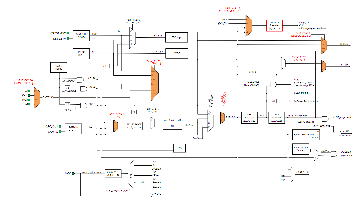
, CFGR4 , :
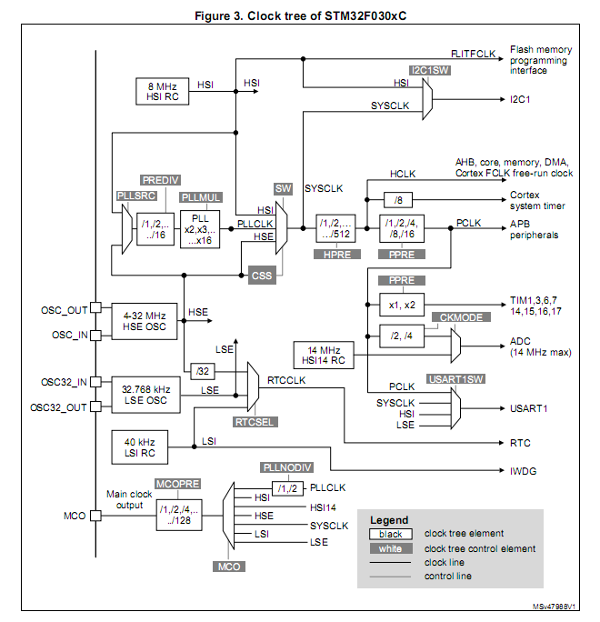
... , STM32F030, CFGR4...
HK32F0_LibraryV1.0.3... :
typedef struct
{
__IO uint32_t CR; /*!< RCC clock control register, Address offset: 0x00 */
__IO uint32_t CFGR; /*!< RCC clock configuration register, Address offset: 0x04 */
__IO uint32_t CIR; /*!< RCC clock interrupt register, Address offset: 0x08 */
__IO uint32_t APB2RSTR; /*!< RCC APB2 peripheral reset register, Address offset: 0x0C */
__IO uint32_t APB1RSTR; /*!< RCC APB1 peripheral reset register, Address offset: 0x10 */
__IO uint32_t AHBENR; /*!< RCC AHB peripheral clock register, Address offset: 0x14 */
__IO uint32_t APB2ENR; /*!< RCC APB2 peripheral clock enable register, Address offset: 0x18 */
__IO uint32_t APB1ENR; /*!< RCC APB1 peripheral clock enable register, Address offset: 0x1C */
__IO uint32_t BDCR; /*!< RCC Backup domain control register, Address offset: 0x20 */
__IO uint32_t CSR; /*!< RCC clock control & status register, Address offset: 0x24 */
__IO uint32_t AHBRSTR; /*!< RCC AHB peripheral reset register, Address offset: 0x28 */
__IO uint32_t CFGR2; /*!< RCC clock configuration register 2, Address offset: 0x2C */
__IO uint32_t CFGR3; /*!< RCC clock configuration register 3, Address offset: 0x30 */
__IO uint32_t CR2; /*!< RCC clock control register 2, Address offset: 0x34 */
uint32_t RESERVED[42]; /*!< Reserved, Address offset: 0x38-dc */
__IO uint32_t HSECTL; /*!< RCC clock HSE control, Address offset: 0xe0 */
uint32_t RESERVED1; /*!< Reserved, Address offset: 0xe4 */
__IO uint32_t CFGR4; /*!< RCC clock control register 4, Address offset: 0xe8 */
__IO uint32_t AHBENR2; /*!< RCC clock configuration ahb, Address offset: 0xec */
} RCC_TypeDef;
... (uint32_t RESERVED[42]; /*!< Reserved) ?
, ! !!! (... USB STM32F0xx...) , :
, STM32F030, :
, STM HK USB ... ... USB ARM, : "NOP
performs no operation and is not guaranteed to be time consuming. The processor might remove it from the pipeline before it reaches the execution stage. " NOP "" ... , ?
ARM!!!
HK "" . .
...
System Tick Timer! , , Watchdog ( - ). , . - :
(STM32F030):
asm_usb_tx
PUSH {R4-R7,LR} ;10
LDR R3,DataTable+0x08 ;6
LDR R2,DataTable+0x14 ;6
STR R2,[R3, #+0x18] ;5
LDR R4,[R3, #+0] ;5
MOVS R5,#+5 ;4
LSLS R5,R5,#+22 ;4
ORRS R5,R5,R4 ;4
STR R5,[R3, #+0] ;5
MOVS R7,#+0 ;4
ADDS R1,R1,#+1 ;4
ut_0
LDRB R5,[R0,#+0] ;5
NOP ;4
NOP ;4
SUBS R1,R1,#+1 ;4
BEQ ut_2 ;4
MOVS R6,#+8 ;4
LDRB R4,[R0,#+0] ;5
ADDS R0,R0,#+1 ;4
"" (HK32F030):
asm_usb_tx
PUSH {R4-R7,LR} ;10
LDR R3,DataTable+0x08 ;6
LDR R2,DataTable+0x14 ;6
STR R2,[R3, #+0x18] ;9 GPIOA->BSRR
LDR R4,[R3, #+0] ;8 GPIOA->MODER
MOVS R5,#+5 ;4
LSLS R5,R5,#+22 ;4
ORRS R5,R5,R4 ;4
STR R5,[R3, #+0] ;6 GPIOA->MODER
MOVS R7,#+0 ;4
ADDS R1,R1,#+1 ;4
ut_0
LDRB R5,[R0,#+0] ;9
NOP ;4
NOP ;4
SUBS R1,R1,#+1 ;4
BEQ ut_2 ;4->8
MOVS R6,#+8 ;4
LDRB R4,[R0,#+0] ;9 Load transmited Byte
ADDS R0,R0,#+1 ;6 Increment TX Buffer Pointer
... LDR/STR Immediate Value... , - - , , - ... , 72 MHz, .
6 9. , , , , "" " ". .
:
...HK STM...
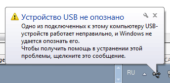
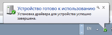
, , STM, , , GPIO. , .
HK , STM, ADC/TIM/USART/IWDG/GPIO, - , , .
72MHz "" / . "" "" . , STM' 48MHz, HK 72, " " 48MHz STM HK 72MHz, 72 != 48, , , .
.
! , .